- #ElectionsWithNewsGram
- HOME
- OPINION
- ON GROUND
- INTERVIEW
- IPL 2026
- INDIA
- NewsGram USA
- WORLD
- न्यूजग्राम
- POLITICS
- ENTERTAINMENT
- CULTURE
- LIFESTYLE
- ECONOMY
- SPORTS
- Jobs / Internships
- Misc.
- NewsGram Exclusive
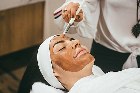
As the world wakes up to clean beauty, a responsible beauty range offers the clarity that new-age consumers crave. Oriflame's Beautanicals range of safe and effective formulations have #NothingToHide. Inspired by Swedish apothecary knowledge and driven by the proven powers of botanical extracts and essential minerals, the brand is going all out in its bid to keep things transparent. Naveen Anand, Senior Director Marketing, South Asia explains how the brand is serving new-age consumers:
How does Beautanical serve new age consumers?
Anand: The current generations — Millennials, GenZ — are more conscious of clean beauty and desire transparency in the products they use. They expect brands to be truthful and conscientious. This is a range of safe, effective and thoughtful formulations which is respectful of nature with #NothingToHide

The current generations — Millennials, GenZ — are more conscious of clean beauty and desire transparency in the products they use. | Photo by Priscilla Du Preez on Unsplash
What are the key ingredients in the skincare range?
Anand: The Beautanicals range is inspired by the pure waters of Scandinavia and driven by the proven powers of botanical extract and 8 essential minerals. It has 95 percent natural origin ingredients, formulated without parabens and silicones, with biodegradable rinse-off formulations and is registered with The Vegan Society. Eight essential minerals found in the pure waters of Scandinavia are crafted into a bespoke blend with Swedish natural honeysuckle extract to bring a range of healthy beauty benefits.
The range comprises thoughtful formulas for beautiful, healthy hair with the Beautanicals Repairing Shampoo and the Beautanicals Repairing Conditioner along with beautifully simple and effective body care with the Beautanicals Repairing Hand Salve and Beautanicals Revitalising Body Cleanser. With essential minerals such as Sodium, Calcium, Zinc, Silica, Copper, Phosphorus, Potassium, Magnesium along with Swedish Natural Honeysuckle extract the range makes hair & body as beautiful as nature intended while restoring your natural beauty from top to toe.
The Beautanicals range is inspired by the pure waters of Scandinavia and driven by the proven powers of botanical extract and 8 essential minerals. | Photo by michela ampolo on Unsplash
How has Oriflame incorporated clean and effective beauty solutions, and what is the key message behind #NothingToHide?
Anand: By #NothingToHide, Oriflame is alluding to the trust and transparency it is building with the new Beautanicals range. This collection of products embodies reliable, clean, and thoughtful formulations that one can trust completely. The ingredients are derived from plants and minerals, the very elements of nature. Moreover, all rinse-off products in the range have been tested for biodegradability and all products are registered with The Vegan Society. Last but not least, we ensured all the bottles are made from 100 percent recycled material, and all-tube packaging contains 55 percent recycled material. Years of focus on holistic beauty has led to this — it truly has nothing to hide and is taking our sustainability accomplishments one step further.
By #NothingToHide, Oriflame is alluding to the trust and transparency it is building with the new Beautanicals range. | Photo by Brooke Lark on Unsplash
Tell us about your key initiatives for sustainability in the Indian market?
Anand: Oriflame is highly committed to environmental protection and sustainability. Over the last decade, we have reduced our environmental impact and use 100 percent renewable energy across all our manufacturing sites and offices. Apart from this, we focus on using biodegradable ingredients in our products to reduce the impact on the planet. In fact, we have banned the use of plastic microbeads & use 100 percent natural exfoliants such as almond shells, fruit seeds & olive stone in our scrub products. Additionally, our wellness factory in India reuses 100 percent of its water & is LEED Gold Certified.
Direct selling is defining self-reliance for Indian women?
Anand: Oriflame's commitment to improving people's quality of life comes from the very opportunity that it creates. With zero investment or fees, women can create their own businesses and fulfil their dreams. Women form an integral part of our journey in India. It presentsthem with a unique, self-actualizing business opportunity — allowing them to earn, build their own business, travel around the world, meet new people and be part of a fun, caring, and friendly global community. Our commitment towards women empowerment also shines through our long-standing association of 15 years with Deepalaya, supporting girl child education.
Oriflame is highly committed to environmental protection and sustainability. | Photo by STIL on Unsplash
What are the key CSR activities that the brand has been working on?
Anand: Oriflame believes that it's best to zero in on one vital area and focus all your energies on it. That's why we have chosen Girl Child Education – an area with a force-multiplier effect and seek to have a real impact there.
The brand's association with Deepalaya started in 2006. This CBSE-affiliated school, with classes till 12th, shares our passion for taking education to the poorest of the poor. To date, we have sponsored the education of over 7,000 girls at Deepalaya. Additionally, we have donated two buses to Deepalaya Learning Centre and also to its schools. Oriflame has also helped Deepalaya construct a three-storey school building in Nuh, one of the most backward districts of Haryana. This school will support providing education to over 3,000 children in the coming years. People, culture and their safety is of prime importance to us. Therefore, during these unprecedented pandemic times, Oriflame, along with Af Jochnick Foundation, has partnered with PHDCCI to donate 2 Oxygen Generation Plants in a bid to ramp up the fight against the Covid-19 pandemic.
What are the markets where Oriflame is witnessing maximum traction?
Anand: India is a key region for us and we have made deep inroads within this highly dynamic market. We have a Pan India presence, covering many pin codes across the length and breadth of the subcontinent. Our strongest markets are East and North-East, followed by the Northern region. Further, the West & South are also key markets for us. (IANS/ MBI)
Keywords: #nothingtohide, natural, products, beauty, beautanicals. oriflame
Subscribe to our channels on YouTube and WhatsApp
Download our app on Play Store